Infrastructure description (distributed in 2 laboratories):
1. Electrical characterization
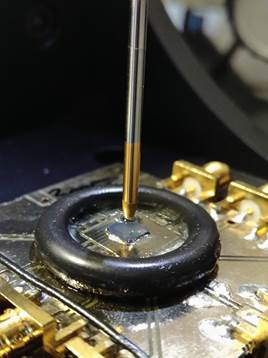
- Manual Probe station (Suss-PM5) with RF-probes up to 40GHz. Dual GSGSG probes with up to 4 signal measurement. Optical microscope for high resolution on-chip measurements. Multi-probe cards.
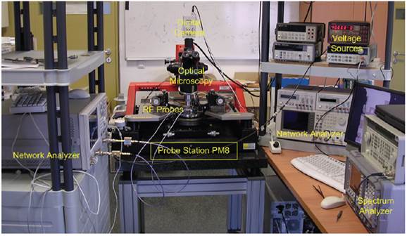
- Agilent Network Analyzer: E5100-A. 10 kHz to 180 MHz;
- Agilent Network Analyzer: E5071B. 300 kHz to 8.5 GHz. 4 ports;
- Agilent semiconductor device analyzer B1500A
- Keysight Signal Analyzer N9030A, 3Hz-3.6GHz
- Agilent Signal Generator: E8847A. 250 kHz to 1 GHz;
- Agilent Pulse Function Arbitrary Generator: 81150A. 1 mHz to 240 MHz. Dual output;
- Agilent high speed Oscilloscope
- Programmable, low-noise and multi-values power supplies
- Vacuum chamber for on-chip characterization
- RF devices (couplers, power splitters, mixers, phase-shifters, amplifiers….)
2. Optical characterization set-up for MEMS resonators
- Optical table with Interferometric HeNe laser vibrometer up to 1GHz. Vacuum/Air operation
3. Acoustic characterization set-up for ultrasound based on
- Hydrophone from Onda Acoustics, 20MHz,
4. Bonding machine
- Wedge and ball wire bonding machine (Al and Au wire) (Kulicke and Soffa)
5. General lab infrastructure
- Optical tables;
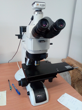
- Optical microscope
- Chemical bench, with N2 availability
- Drying oven. 80 litres, 250 ºC
6. Software
- For MEMS design and analysis: COMSOL and COVENTOR
- For Integrated circuit design (CADENCE)